ADL5317
Rev. 0 | Page 9 of 16
THEORY OF OPERATION
The ADL5317 is designed to address the need for high voltage
bias control and precision optical power monitoring in optical
systems using avalanche photodiodes. It is optimized for use
with the Analog Devices, Inc. family of translinear logarithmic
amplifiers that take advantage of the wide input current range
of the ADL5317. This arrangement allows the anode of the
photodiode to connect directly to a transimpedance amplifier
for the extraction of the data stream without need for a separate
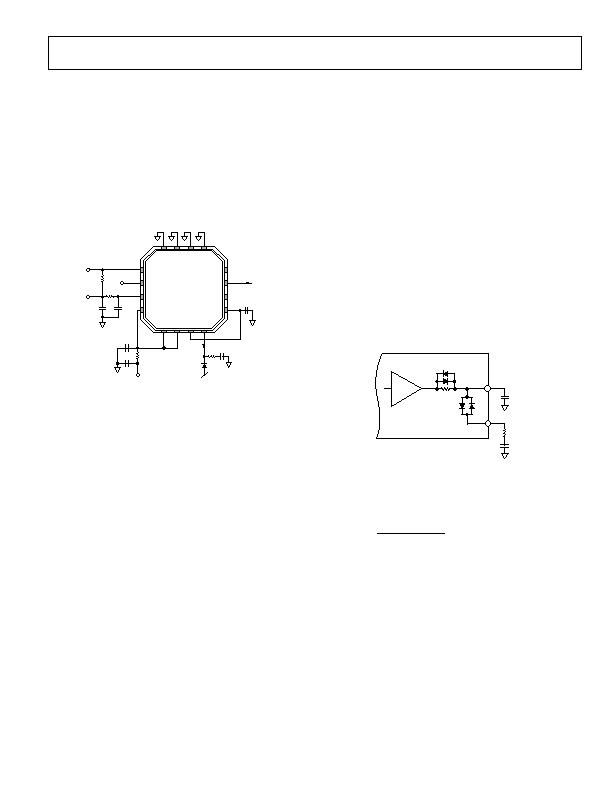
optical power monitoring tap. Figure 19 shows the basic
connections for the ADL5317.
1
FALT
2
V
SET
3
4
11
IPDM
12
NC
10
NC
9
GARD
5
6
7
8
15
16
14
13
ADL5317
FALT
VSET
VPLV
VPHV
MIRROR CURRENT
OUTPUT
0.01?/SPAN>F
APD
1nF
1k?/SPAN>
I
APD
0.1?/SPAN>F
0.01?/SPAN>F
HIGH VOLTAGE
SUPPLY
0?/SPAN>
LOW VOLTAGE
SUPPLY
10k?/SPAN>
0?/SPAN>
0.01?/SPAN>F
0.1?/SPAN>F
Figure 19. Basic Connections
At the heart of the ADL5317 is a precision attenuating current
mirror with a voltage following characteristic that provides
precision biasing at the monitor input. This architecture uses a
JFET-input amplifier to drive the bipolar mirror and maintain
stable V
APD
voltage, while offering very low leakage current at
the VAPD pin. The mirror attenuates the current sourced
through VAPD by a factor of 5 to limit power dissipation under
high voltage operation and delivers the mirrored current to the
IPDM monitor output pin. Proprietary mirroring and cascoding
techniques maintain the linearity vs. the input current and
stability of the mirror ratio over a very wide range of supply and
V
APD
voltages.
BIAS CONTROL INTERFACE
In the linear operating mode, the voltage at VAPD is referenced
to ground, and follows the simplified equation
V
APD
= 30 ?V
SET
GARD is driven to the same potential as VAPD for use in
shielding the highly sensitive VAPD pin from leakage currents.
The GARD and VAPD pins are clamped to within approxi-
mately 40 V below the VPHV supply to prevent internal device
breakdowns, and VAPD is clamped to within a volt of GARD.
The VAPD adjustment range for a given high voltage supply,
VPHV, is limited to approximately 33 V (or less, for V
PHV
<
41 V). For example, VAPD is specified from 40 V to 73.5 V for
a 75 V supply, and 6 V (the minimum allowed) to 28.5 V for a
30 V supply. When VAPD is driven to its lower clamp voltage
via the VSET pin, the mirror can continue to operate, but the
VAPD bias voltage no longer responds to incremental changes
in VSET.
GARD INTERFACE
The GARD pins primarily shield the VAPD trace from leakage
currents and filter noise from the bias control interface. GARD
is driven by the VSET amplifier through a 20 k?resistor. This
resistor forms an RC network with an external capacitor from
GARD to ground that filters the thermal noise of the amplifiers
feedback network and provides additional power supply
rejection. The series components, RCOMP and CCOMP, shown in
Figure 20, are necessary to ensure essential high frequency
compensation at the VAPD input pin over the full operating
range of the ADL5317.
V
SET
AMPLIFIER
GARD
C
GRD
ADL5317
X30
VAPD
C
COMP
R
COMP
20k?/SPAN>
Figure 20. Filtering VAPD Using the GARD Interface
The cutoff frequency of the GARD interface for small signals
and noise is defined by
GRD
3dB
C
F
?/DIV>
?/DIV>
=
k?/DIV>
20
2?/DIV>
1
where:
F
3dB
is the cutoff frequency of the low-pass filter formed by the
on-board 20 k?and C
GRD
.
C
GRD
is the filter capacitor installed from GARD to ground.
A larger value for C
GRD
(up to approximately 0.01 糉) provides
superior noise performance at the lowest input current levels,
but also slows the response time to changes in VSET.
The pull-up of the VSET amplifier is limited to approximately
2.5 mA, resulting in a slew limited region for large signals,
followed by an RC decay for the final 700 mV. This decay
corresponds to the above single-pole equation. The pull-down
of the V
SET
amplifier is largely resistive, equivalent to
approximately 90 k?in parallel with 70 糀 to ground.
发布紧急采购,3分钟左右您将得到回复。
相关PDF资料
ADM1027ARQZ-RL7
IC REMOTE THERMAL CTLR 24QSOP
ADM1029ARQZ-R7
IC SENSOR 2TEMP/FAN CTRL 24QSOP
ADM1030ARQZ-RL7
IC SNSR TEMP/FAN PWM CTRL 16QSOP
ADM1032ARZ-REEL
IC TEMP MONITOR 85DEG 8SOIC
ADM1033ARQZ-RL7
IC THERM/FAN SPEED CTLR 16-QSOP
ADM1034ARQZ-REEL
IC THERM/FAN SPEED CTRLR 16-QSOP
ADN8810ACPZ-REEL7
IC CURRENT SOURCE(12BIT) 24LFCSP
ADP2140ACPZ3328R7
IC REG DL BCK/LINEAR 10LFCSP
相关代理商/技术参数
ADL5317ACPZ-WP
制造商:Analog Devices 功能描述:SP Amp LOG Amp Single 6V/80V 16-Pin LFCSP EP Tray 制造商:Analog Devices 功能描述:SP AMP LOG AMP SGL 6V/80V 16LFCSP EP - Bulk
ADL5317-EVAL
制造商:Analog Devices 功能描述:EVAL BD FOR AVALANCHE PHOTODIODE BIAS CNTRLR AND WIDE RANGE - Bulk
ADL531A-53M0
制造商:Panasonic Industrial Company 功能描述:VALVE
ADL5320
制造商:AD 制造商全称:Analog Devices 功能描述:400 MHz to 2700 MHz RF Driver Amplifier
ADL5320_08
制造商:AD 制造商全称:Analog Devices 功能描述:400 MHz to 2700 MHz RF Driver Amplifier
ADL5320ARKZ
制造商:Analog Devices 功能描述:AMP DVR RF 400MHZ-2.7GHZ 3SOT89 制造商:Analog Devices 功能描述:AMP, DVR, RF, 400MHZ-2.7GHZ, 3SOT89 制造商:Analog Devices 功能描述:AMP, DVR, RF, 400MHZ-2.7GHZ, 3SOT89; Frequency Min:400MHz; Frequency Max:2.7GHz; Gain:17dB; Noise Figure Typ:5.1dB; RF IC Case Style:SOT-89; No. of Pins:3; Supply Voltage Min:4.5V; Supply Voltage Max:5.5V; RF Type:Broadband; ;RoHS Compliant: Yes
ADL5320ARKZ-R7
功能描述:IC AMP RF DRIVER 2.7GHZ SOT89 RoHS:是 类别:RF/IF 和 RFID >> RF 放大器 系列:- 标准包装:3,000 系列:- 频率:100MHz ~ 6GHz P1dB:9.14dBm(8.2mW) 增益:15.7dB 噪音数据:1.3dB RF 型:CDMA,TDMA,PCS 电源电压:2.7 V ~ 5 V 电流 - 电源:60mA 测试频率:2GHz 封装/外壳:0505(1412 公制) 包装:带卷 (TR)
ADL5320ARKZ-WP
制造商:AD 制造商全称:Analog Devices 功能描述:400 MHz to 2700 MHz Pre-driver RF Amplifier